
close
Choose Your Site
Global
Social Media


| Layer | 2L |
| Base Material | Copper |
| Specification | PCB customized size |
| Delivery | 7-14 Days |
| Certification | UL(CUL), IS09001&IS014001, IATF16949, REACH, RoHS, |
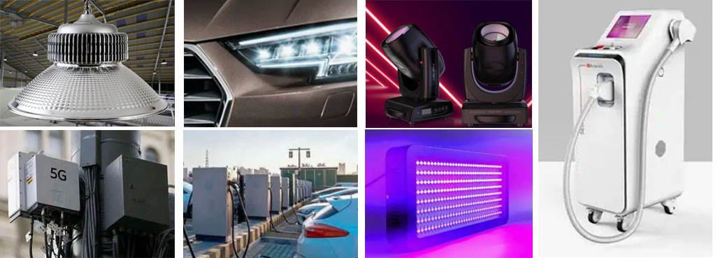
| Application | Automotive Headlights, New Energy, Charger, Stage Lighting, Outdoor Lighting, 5G equipment driver, inverter, UV Curing |
| Transport Package | Vacuum Package and Foam Protected |
| Surface treatment | OSP / Immersion Nickel Gold / Immersion Nickel Palladium Gold / Immersion Tin / HASL |
| Product Thickness min./max. | 0.6/3.2 |
Minimum Dielectric Layer Thickness | 38μm |
Maximum Outer Layer Copper Thickness | 15oz |
| Minimum Outer Layer Line Width/Gap | 0.1/0.1mm |
| Minimum Mechanical Hole Diameter | 0.6mm |
| Minimum Solder Mask Ring Width | 0.05mm |
| Minimum Solder Mask Window | 0.025mm |
| Minimum Pad to Window Tolerance | 0.05mm |
| Minimum Hole to Window Tolerance | 0.05mm |
| Minimum Milling Depth Tolerance | 0.035mm |
| Hole to Pad Tolerance | 0.035mm |
| Hole to Hole Tolerance | 0.035mm |
| Dielectric Layer Thermal Conductivity(w/m.k) | 380.0W-400.0W, Breakdown Voltage: 2KV - 6KV |
Our copper-based heat sink products utilize advanced welding and lamination technology, ensuring a tight bond with the heat sink. This significantly improves the heat dissipation efficiency of the equipment and greatly reduces subsequent assembly and processing costs, making it a professional and efficient integrated copper-based heat sink solution.
Our Reliable Material Suppliers

Our Product Features
1. Single-sided double-layer copper foil. Directly receives heat from components, resulting in a shorter heat conduction path and a 30%-50% increase in heat dissipation area. Heat dissipation efficiency is 2-3 times higher than ordinary aluminum substrates with heat sinks.
2. Low thermal resistance. Overall thermal resistance can be as low as 0.1-0.5℃/W, effectively controlling the junction temperature of high-power devices and preventing light decay, shortened lifespan, or performance failure due to overheating.
3. Strong structural stability, adaptable to complex working environments. Warpage deformation is reduced by more than 60%.
4. Integrated heat sink design improves reliability. The copper substrate and heat sink are bonded together by welding, pressing, or thermal adhesive, resulting in a tight fit with no gaps or dead zones for heat conduction. Compared to solutions that add heat sinks later, this design offers stronger shock resistance.
5. High circuit design flexibility, adaptable to single-sided high-density layouts. The single-sided double-layer copper foil has clear functional partitions: the upper copper foil is the circuit layer, allowing for high-density circuitry and pad design, supporting SMT. The lower copper foil layer is a dedicated thermally conductive layer, not involved in circuit transmission, only responsible for heat dissipation, avoiding the limited circuit layout issues caused by "circuit and heat dissipation sharing a single copper layer".
6. Compatible with high-current scenarios. The double-layer copper foil has a stronger current-carrying capacity; a single square millimeter of copper foil can carry 5-8A of current, suitable for high-current circuit designs in new energy power modules and high-power drive power supplies, while reducing heat loss in the circuit.
7. Balanced cost and performance, with a cost-effectiveness superior to pure ceramic substrates. Furthermore, the processing technology is more mature.
8. Adaptable to high-power lighting. Improved beam uniformity and better heat dissipation uniformity avoid LED color temperature drift and uneven beam brightness caused by localized overheating.
9. Significantly extended lifespan: Through precise temperature control, the lifespan of high-power lighting products can be extended to over 50,000 hours, far exceeding that of ordinary aluminum substrate solutions.
Applications
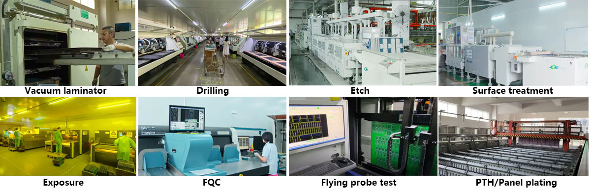
Our Strong Production Capacity
Our Customers Reference

FAQ
Q1: Where are you headquartered?
Foshan, China(south of China)
Q2: Are you a trading company or manufacturer?
We are a PCB&PCBA manufacturer with 10+ years experiences.
Q3: What countries do you export your products to?
We export our PCB/PCBA solutions to more than 30 countries, including USA,EUROPE,MIDDLE EAST,AUSTRALIA,AGENTINA,BRAZIL and so on.
Q4: What is your lead time/production time?
1-3 weeks
Q5:Do you offer free samples?
Free in 3 new models
Q6:What's your MOQ?
100pcs
Q7:How's your quality control?
We have 100% unit inspection, process:
Strictly Select Suppliers->IQC->IPQC->ICT->AOI TEST->X-ray Test->Function Test
1.Thermal Performance Testing
2.Electrical Testing(Hi-Pot Test / Dielectric Withstanding Voltage, Dielectric Breakdown Voltage, Continuity & Short Test)
3.Mechanical Testing
4.Surface & Process Testing
Our Company Profile
Guoli Optoelectronics has more than 10 years experiences in PCB, PCBA design and manufacturing, copper base PCB application, we have strong engineers team for software and hardware development, and with 50+ patents in PCB products. We have 4 manufacturing bases and 600+ staffs, strong production capacity and fast response to make sure your project run efficiently. We have thousands of successful customers and cases globally, and serving the brands in industry worldwide.
We have complete quality control system and management system to keep our product quality, including UL, Rohs, ISO9001, ISO14001 and IATF16949.
Our Advantages
1. Save Time and Costs: GUOLI provides PCB design, sourcing, assembly, testing, and after-sales services, reducing communication and delivery time with different suppliers, improving efficiency, and lowering costs.
2. Reduce Errors: PCB design and assembly defects can cause project delays. GUOLI's one-stop PCBA service reduces various errors, including design, sourcing, and assembly mistakes, thereby improving quality control.
3. Strong Technical Team: GUOLI's one-stop PCBA service is typically equipped with an experienced technical team to help customers solve various technical problems and ensure timely project completion.
4. Unified Warranty and After-Sales Service: GUOLI's one-stop PCBA service provides unified warranty and after-sales service, helping to build long-term partnerships and achieve mutual benefit.
5. Customized Services: GUOLI's one-stop PCBA service can provide more personalized services based on customers' specific needs and requirements, and develop suitable circuit boards and system components.


